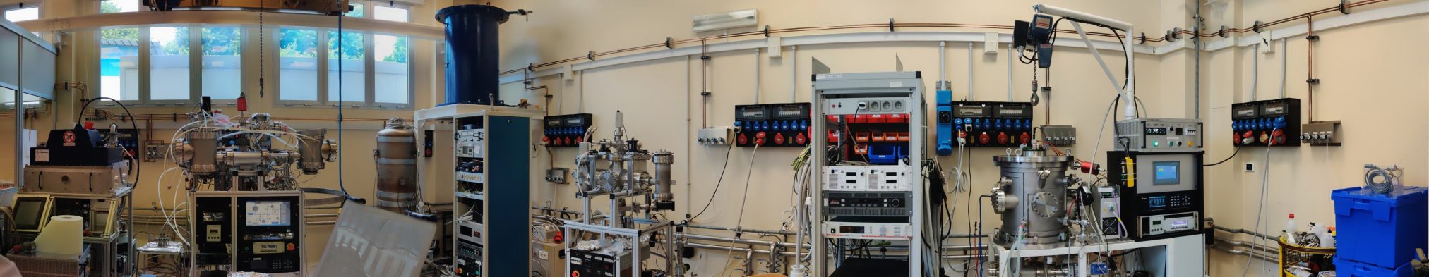
PVD Facility @Laboratori Nazionali di Legnaro, PD
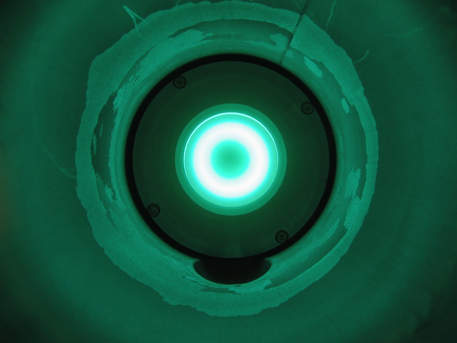
Sputtering is a PVD technique (Physical Vapor Deposition), a low temperature process where a plasma is generated in vacuum, in order to bombard the target connected to the negative electrode of an electric power supply with positive ions. The target is vaporized and the vapours are deposited on the substrate creating a thin atomic layer over atomic layer. The Sputtering technique allows the deposition of thin films of any material on a substrate of a second material, with practically infinite applications ranging from high temperature superconducting films to hard coatings for cutting tools, from films that limit the secondary ionization of the surfaces to the materials used in thermodynamic panels.
An important advantage of sputter deposition is the high purity of the coatings grown, possible due to the Sputtering process is developed in vacuum. Sputter films have a composition close to the source material (target), even materials and compounds with very high melting points are easily sputtered.
This technique is used for growing for examples:
- Superconductive coating like in LNL QWRs
- Protective coating capable of resisting corrosion by liquid metal: the thin film developed is capable of reducing the wettability of the corrosive liquid on the surface to be protected.
- Decorative coating: for example, 24-karat gold films can be made of precious materials on less noble materials such as plastic, wood and textiles.
- Functional coating: The tools used for cutting hard materials, protection of solar panels, functionalization of surfaces.
- Metallized plastic meshes, used in the cellular and smartphone industry, which act both as a faraday cage and as protection for audio speakers.
It is a very versatile technique but difficult to standardize, so it is necessary to create a system custom-made for the required application, able to optimize the process and the results.
If it is necessary to cover large surfaces with thin films or flexible substrates in large quantities, the PVD technique can be used in a semi-continuous process (called Roll to Roll) by depositing on rolls even hundreds of meters in systems that are called web coatings capable of depositing thin films on aluminium rolls used for examples in the solar thermal industry.
In the field of Physical Vapor Deposition (PVD) treatments, the Legnaro facility focuses its work on metallic thin films deposition over a wide range of different surfaces by means of magnetron sputtering techniques, HiPIMS and Plasma Enhanced CVD. The Legnaro activities include the optimization of manufacturing techniques for superconductive accelerating cavities and other technology transfer activities such as solar mirrors and panels, hard and protective coating, getter materials and anti-reflective coating the production of metallic coating but also oxide, nitride, carbide and carbonitride. In addition, the vacuum brazing technique is applied for the manufacturing of resisting coatings, diamonds-based, for cutting tools, avoiding the electrochemical process that uses Nickel.
The laboratories are equipped with various PVD (sputtering and cathodic arc) and PECVD systems capable of performing the most varied coatings (metallic and not only) on surfaces even of considerable size.
The service is also equipped with different analysis techniques optimized for thin films characterization such as XRD, SEM, profilometry, etc.